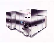
Low cost, high throughput EBDW system writes circuits of 65nm and smaller
The F3000 is an EB lithography system optimized for system LSIs of 65nm and smaller, supporting 300 wafer process technology, that offers shorter TATs in high-mix, variable-volume production environments.
Inheriting the high-resolution electron optical technology, the reliability, and the high average operation rate of previous models, the F3000 also boasts a more rigid body and upgrades to every aspect of its functionality, leading to significant improvements in image placement accuracy.
As a further measure to enhance lithographic processing capacity and pattern characteristics, the F3000 is equipped with an upgraded CP exposure function.
- Ideal for writing system LSIs in high-mix, variable-volume production environments
- High resolution, high accuracy, high throughput
- Supports 300mm wafers
- Offers full & partial CP exposure functionality
- Self-cleaning technology
| Supported Wafer Size | 300mm |
|---|---|
| EB Acceleration Voltage | 50kV |
| Lithography Methods | CP, VSB |
| Reduction Ratio of CP Projection | 60x |
| Supported Nodes | 65nm |


